

UNIVERSITY EXAMINATIONS: 2020/2021
EXAMINATION FOR THE DEGREES OF BACHELOR OF SCIENCE
IN INFORMATION SECURITY & FORENSICS
BISF 1208: SEMICONDUCTORS AND DIGITAL ELECTRONICS
FULLTIME/ PART TIME/DISTANCE LEARNING
ORDINARY EXAMINATION
DATE: DECEMBER, 2021 TIME: 2 HOURS
INSTRUCTIONS: Question ONE IS COMPULSORY, Choose TWO OTHER Questions
QUESTION ONE
(a) State:
i. Two ways of ionizing an atom
ii. Two advantages of silicon over germanium diodes
(4 Marks)
(b) Define the following with respect to semiconductors:
i. Covalent bond
ii. Drift current
(4 Marks)
(c) With the aid of a labelled diagram, describe the formation of depletion layer at the
P-N junction.
(7 Marks)
(d) Figure 1 shows a diagram of an N- type material of resistance 2 KΩ connected
across a 15V d.c supply.
Figure 1

i. Redraw the diagram showing the direction of electrons and holes inside the
material
ii. Taking the electronic charge, e=1.6 X 10⁻¹⁹ C, determine the
I. Current through the material
II. Number of electrons passing through a given point per second
N- TYPE MATERIAL
III. Electrical energy expended if the current is maintained for
30Ms
(9 Marks)
(e) Draw the circuit of a common collector configuration of a transistor amplifier.
(6 Marks)
QUESTION TWO
(a) Define the following
i. Transistor biasing
ii. Transistor saturation
iii. Feedback current
(3 Marks)
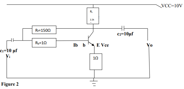
Figure 2
(b) Figure 2 shows a circuit diagram of an amplifier using the collector base feedback
biasing.
Taking β=50 and Vbe=0.7V, determine the:
i. Base current Ib;
ii. Collector current Ic:
iii. Collector emitter voltage, Vce
(9 Marks)
(c) Sketch the transfer characteristic curve for a common emitter transistor.
(3 Marks)
QUESTION THREE
(a) State three(3) advantages and disadvantages of FETs.
(6 Marks)
(b) Using a diagram of a CMOS voltage multiplier circuit:
i. Explain its operation
ii. Sketch the output wave form, when subjected to sinusoidal wave form at the input
iii. State three applications of this circuit
(9 Marks)
QUESTION FOUR
(a) Draw a well labelled diagram of half wave regulated power supply and explain the
function of each component used
(6 Marks)
(b) A full wave bridge rectifier is supplied from a transformer whose secondary voltage is
60Vrms.
Determine the:
i. Peak value of the secondary voltage:
ii. DC voltage of the rectifier output;
iii. Ripple factor.
(9 Marks)
QUESTION FIVE
(a) State three:
i. Components of sinusoidal wave.
ii. Biasing methods of bipolar junction transistor (BJT)
(6 Marks)
(b) A sinusoidal wave of 50Hz with maximum voltage of 10V for a period of 2nS.
Determine:
i. Its instantaneous voltage
ii. Time t when frequency shifted to 100Hz
iii. Its instantaneous voltage at t=2µs in (b)ii above
(9 Marks)